About our lab
The Reference laboratory was established at the Faculty of Electrical Engineering of CTU in 2023 as part of the international TACOM project. Within this project, Prof. Bohuslav Rezek's group at the Department of Physics partners with the NenoVision company for the research and development of new methods of correlative microscopy using atomic force microscopy (AFM) and scanning electron microscopy (SEM). The combination of both methods is referred to as correlative probe-electron microscopy (CPEM). This method combines the signal from AFM and SEM microscopes into a final comprehensive data set and visualization, correlating selected morphological, chemical, mechanical, electrical and magnetic properties. Applications of this method range from life sciences to semiconductor and nanomaterial analysis. The Reference laboratory is used for demonstration and trial measurements in CPEM mode. In addition to this method, the laboratory also houses instruments for other correlative measurements, such as a multifunctional micro-spectrometer that includes Raman spectrometer, photoluminescence spectrometer, atomic force microscope, Kelvin probe microscope and scanning near-field optical microscope (SNOM). We also use scanning Kelvin probe (SKP) and ambient photoemission spectroscopy (APS) system. The Reference laboratory is open to anyone interested in trying the correlative measurements. In case of interest, feel free to use the contact form.
Highlights
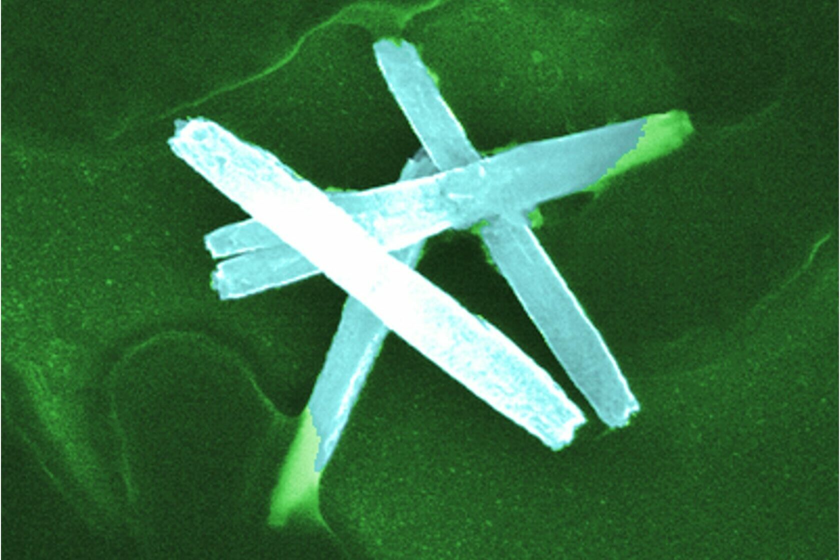
ZnO nano-needles with bacteria
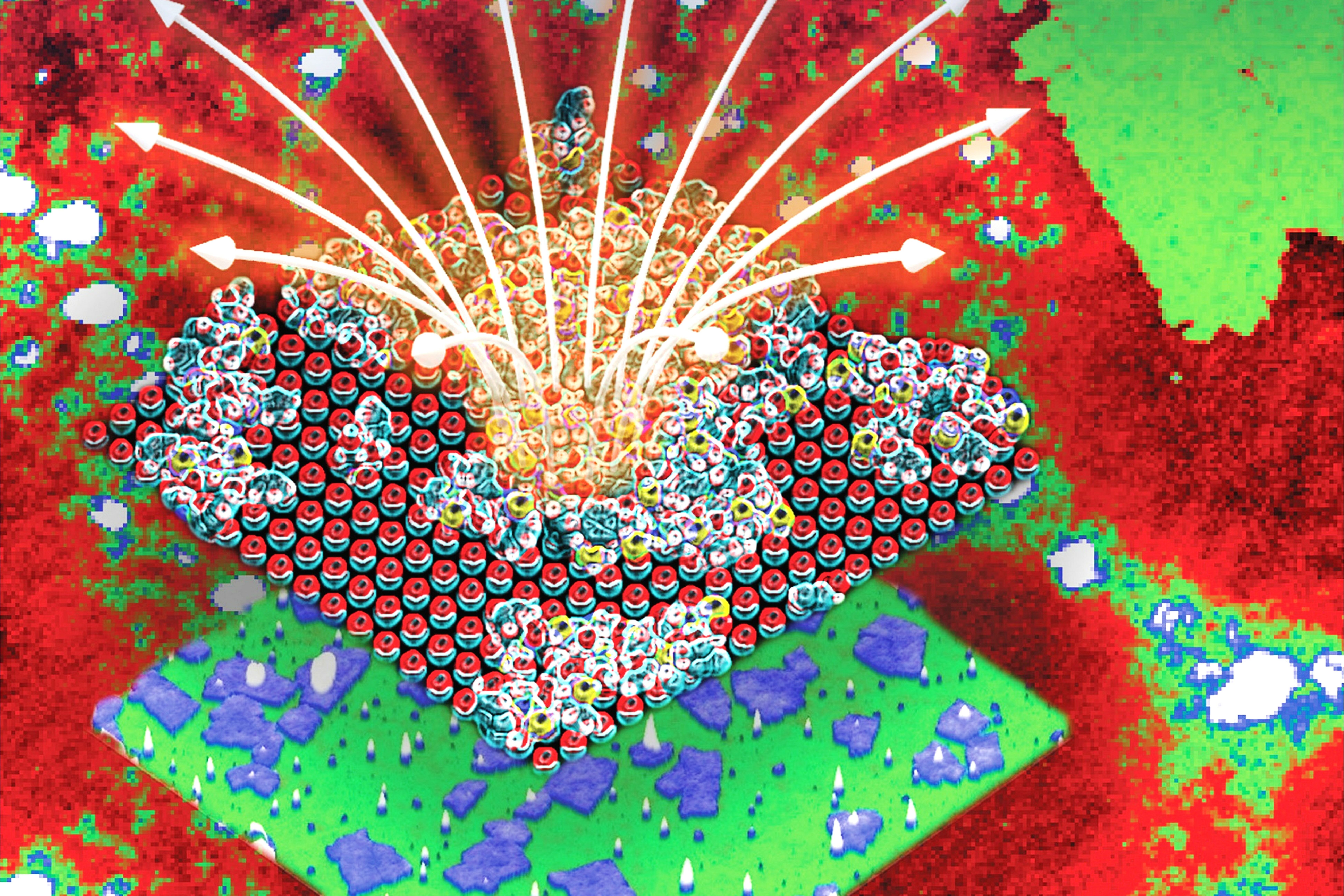
arrangement of drug molecules by surface dipole
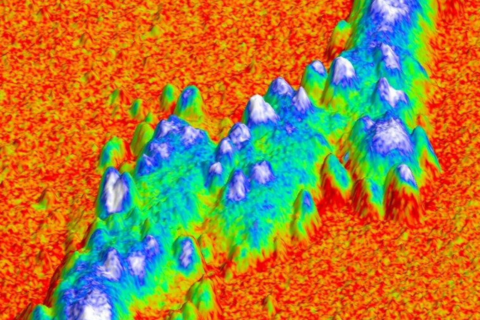
bacteria covered by nanodiamonds and silver
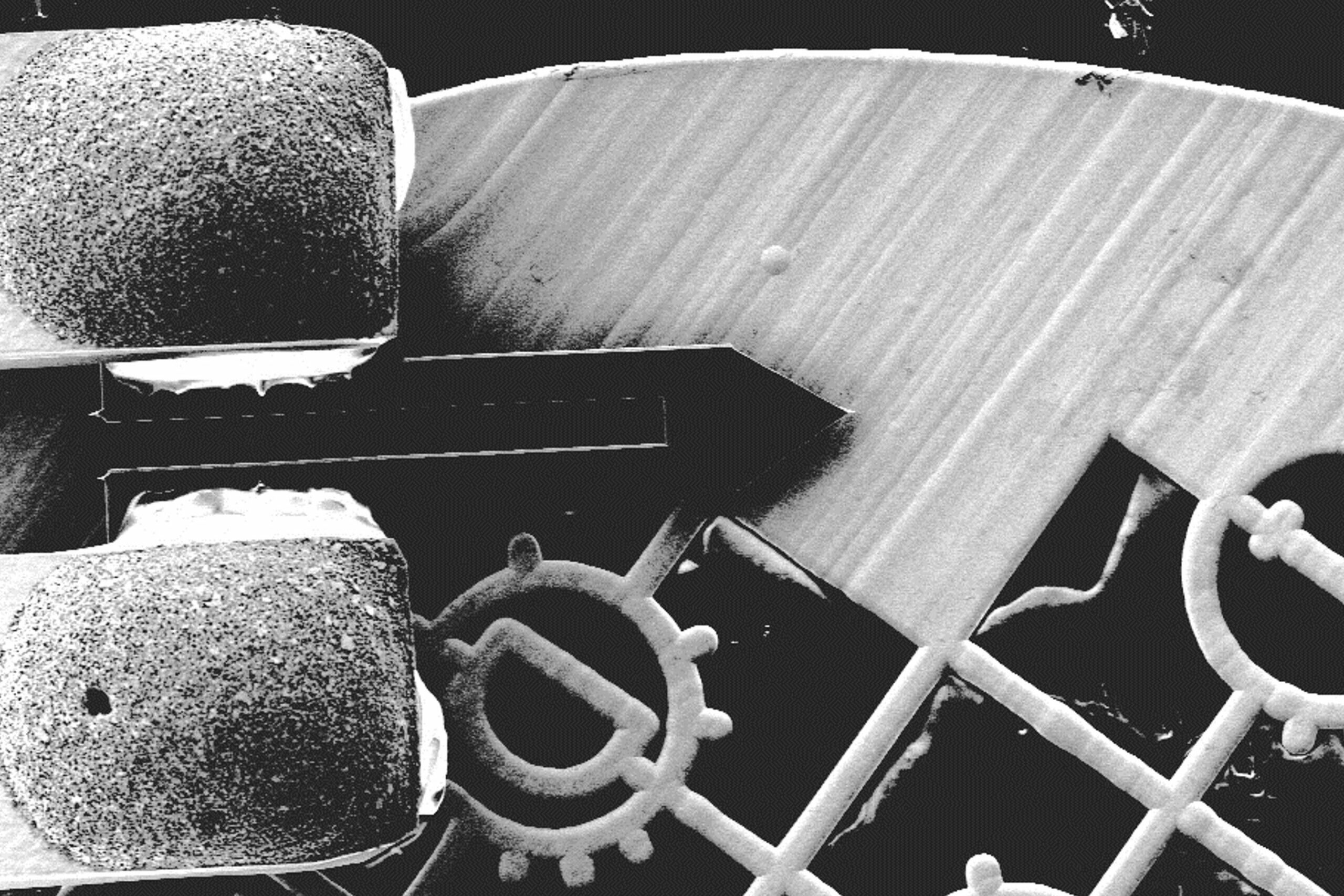
self-sensing probe on a registration grid
Related Publications
[1] Correlative atomic force microscopy and scanning electron microscopy of bacteria-diamond-metal nanocomposites. [https://doi.org/10.1016/j.ultramic.2023.113909]
[2] AFM-in-SEM analyses of thiorphan assembly on ZnO polar and nonpolar surfaces. [https://doi.org/10.37904/nanocon.2023.4761]
[3] Correlative probe microscopy analysis of plasma-treated gallium-doped zinc oxide nanorods. [https://doi.org/10.37904/nanocon.2023.4762]
[4] AFM-in-SEM analysis on heterostructure edges of graphene and hexagonal boron nitride. [https://doi.org/10.37904/nanocon.2023.4810]
How does CPEM work?
Correlative microscopy combining AFM and SEM (CPEM) takes advantage of both methods to obtain a more comprehensive view of the sample under investigation. Using AFM, we can obtain a highly accurate 3D map of the surface height profile and other information in advanced atomic force microscopy modes. SEM gives us a quick view of the surface morphology and other information about the local electronic properties and composition of the sample, including the chemical groups on the surface. It also helps us to more quickly find an area suitable for detailed investigation. The selected area is then imaged by both instruments simultaneously (and therefore under the same conditions), resulting in comprehensive correlated data that maps various properties of the sample and makes their interrelationships visible. You can find out more about the method directly on the company's website (NenoVision).


Project TM03000033
Contact
Form for CPEM demonstration and testing on your own samples can be found here:
Where to find us
Department of physics, FEE CTU, Technická 2, 160 00, Prague 6